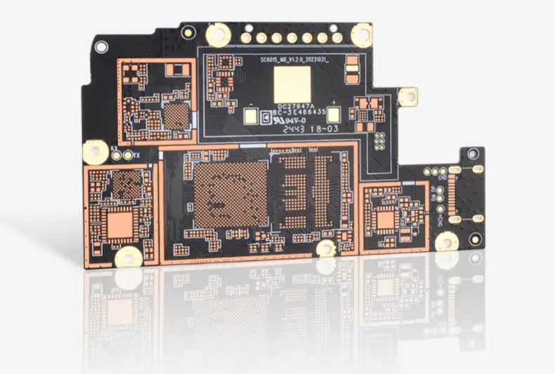
1. The Microvia Minefield: Don’t Let Small Features Cause Big Failures
Microvias are the heart of HDI technology, enabling dense interconnections. However, pushing their limits without considering process capabilities is a common misstep.
The Risk: Excessively high aspect ratios or insufficient copper plating in stacked and staggered vias can lead to plating voids, poor reliability, and intermittent field failures that are notoriously difficult to diagnose.
Our Recommendation: Adhere to a maximum aspect ratio of 0.8:1 for laser-drilled microvias. Collaborate early with your manufacturer to define their proven, reliable design rules for via size, pad diameter, and copper plating specifications to ensure long-term robustness.
2. The Alignment Imperative: When Registration Tolerances Make or Break Your Board
In HDI designs, where trace and space measurements are down to a few mils, layer-to-layer misalignment is the silent killer of yield.
The Risk: A design that doesn’t account for manufacturing registration tolerances can result in broken connections, short circuits, and non-functional boards. Designs operating at the absolute limit of the process window have a high probability of failure.
Our Recommendation: Always design with your fabricator’s registration capability in mind (e.g., ±0.025mm). Incorporate fiducial marks and clear polarity indicators on every layer. Avoid “as-tight-as-possible” feature placements and build in a comfortable margin for error.
3. The Balance Factor: Preventing the Warpage Nightmare
The intricate, asymmetric copper patterns common in HDI can create significant stress during the lamination process.
The Risk: Uneven copper distribution across layers creates differential expansion and contraction, leading to board warpage. This causes issues in assembly (poor solder paste printing, component misalignment) and can even lead to delamination or cracked vias.
Our Recommendation: Use uniform copper pours and thieving patterns in large, empty areas to balance copper density across the layer stackup. Consult with your manufacturer early for their preferred fill patterns and stack-up symmetry guidelines to ensure a flat, stable board.
We Want to Hear From You
Which of these challenges has been the trickiest in your HDI projects? Was it via reliability, layer alignment, or managing board stress? Share your experience in the comments below!
Looking for a Partner, Not Just a Vendor?
If you’re seeking a manufacturing partner that provides expert DFM analysis and guidance from the very first design review, we’re here to help.
Send us a message with “HDI DFM” to start a conversation about optimizing your next design for success.
#HDIDesign #PCBManufacturing #DFMTips #HardwareEngineering #PCBA #Electronics #Tech #Innovation #Engineering